Breakthrough Innovations in EUV Technology Could Slash Smartphone Prices and Power Usage
2024-09-29
Author: Nur
Introduction
In an exciting development for the tech world, MediaTek's latest Dimensity 9400 application processor boasts an incredible density of 30 billion transistors, highlighting the growing need for advanced manufacturing technologies. At the heart of this evolution is extreme ultraviolet lithography (EUV), a cutting-edge technique that enables chip makers to etch minuscule patterns on silicon wafers with precision greater than a human hair.
The Current Landscape of EUV Technology
Currently, Dutch company ASML stands as the sole supplier of these pioneering EUV machines, and their second-generation models, known as High-NA, come with a hefty price tag of around $400 million. These machines allow semiconductor foundries to produce integrated circuits with a process node of 7nm and smaller. The significant investment required to establish a semiconductor fabrication plant translates into higher costs for manufacturers, which ultimately impacts consumers at checkout.
A Revolutionary Innovation
However, a groundbreaking innovation from the Okinawa Institute of Science and Technology (OIST) could revolutionize this landscape. Researchers led by professor Tsumoru Shintake have designed a new, low-cost EUV system that dramatically cuts down on manufacturing expenses and energy consumption—potentially paving the way for reduced smartphone prices.
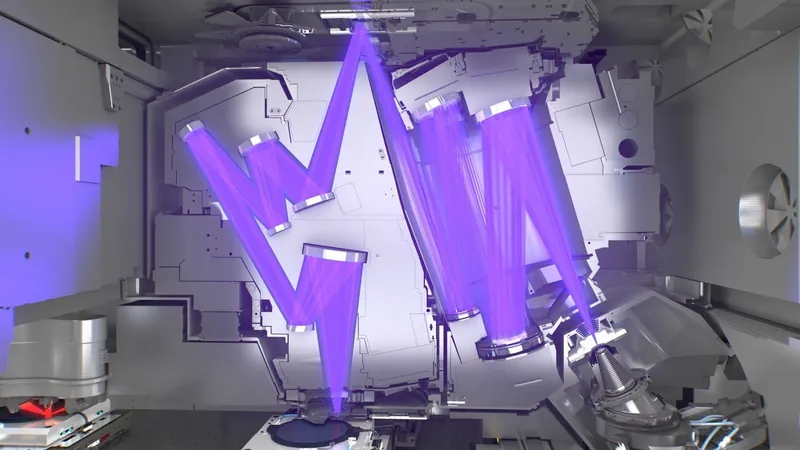
Key Advancements in the New EUV System
One of the key advancements is the reduction in the number of reflective mirrors used in the EUV process, from ten to just four. This new design consumes only 10% of the power of traditional EUV machines. The creative optical projection system relies on only two mirrors, directing light more efficiently onto the silicon wafer without obstructing its path. Professor Shintake describes this innovation as a “breakthrough technology,” claiming it can eliminate challenges previously thought to be insurmountable in EUV lithography.
Efficiency and Cost-Effectiveness
Since EUV rays possess extremely short wavelengths, they cannot traverse transparent lenses, so current systems utilize a series of crescent-shaped mirrors, leading to energy loss as light bounces along its path. Shintake’s approach aligns two mirrors with tiny holes in a straight line, significantly enhancing efficiency. Traditional EUV setups demand upwards of 1 megawatt (MW) of power and capital investments over $200 million, whereas the new low-cost alternative operates on less than 100 kilowatts (kW) and requires an investment below $100 million. Additionally, while typical EUV machines need a light source exceeding 200 watts, the innovative model only requires a mere 20 watts.
Implications for the Semiconductor Industry
Fewer mirrors not only reduce costs but also mitigate energy loss—each reflective bounce results in a 40% decrease in EUV energy. By restricting the light’s journey to four mirrors, more than 10% of the energy can be effectively utilized, allowing lower-wattage sources to function efficiently. The compelling implications of this discovery could lead to significant leaps in power efficiency across the manufacturing spectrum.
Patent and Future Outlook
OIST has already filed a patent for this revolutionary EUV technology, raising questions about its potential impact on global semiconductor dynamics. Particularly, if granted, it could influence ongoing restrictions on Chinese foundries that currently face hurdles in accessing advanced EUV machinery—an issue crucial for companies like Huawei, which struggle to source processors built with nodes smaller than 7nm due to these limitations.
Conclusion
Looking ahead, Professor Shintake emphasizes the promising economic opportunities this innovation could unlock, forecasting that the global EUV lithography market is projected to expand from $8.9 billion in 2024 to $17.4 billion by 2030, at an average annual growth rate of about 12%. If successful, these breakthroughs not only have the potential to make smartphone technology more affordable for consumers but could also herald a new era of energy-efficient manufacturing practices across the entire semiconductor industry. Stay tuned, as the future of smartphone pricing could be closer than we think!


 Brasil (PT)
 Canada (EN)
 Chile (ES)
 España (ES)
 France (FR)
 Hong Kong (EN)
 Italia (IT)
 日本 (JA)
 Magyarország (HU)
 Norge (NO)
 Polska (PL)
 Schweiz (DE)
 Singapore (EN)
 Sverige (SV)
 Suomi (FI)
 Türkiye (TR)