Revolutionary Discovery: Creating Ultra-Thin Hexagonal Boron Nitride for Next-Generation Electronics!
2024-12-02
Author: Sophie
Introduction
In a groundbreaking advancement for the electronics industry, an international team of scientists led by Xixiang Zhang from KAUST has developed a novel method to produce high-quality insulating films of hexagonal boron nitride (hBN) that are merely one atom thick. This incredible feat promises to revolutionize the manufacturing of electronic devices on an industrial scale, marking a significant leap forward in the capabilities of two-dimensional materials.
Significance of Hexagonal Boron Nitride
Published in the prestigious journal Nature Communications, this research highlights the potential of hexagonal boron nitride, a material crucial for semiconductor devices. It plays a vital role in enhancing the performance of other 2D materials, including graphene and transition metal dichalcogenides (TMDs), which are key components in the latest advancements in quantum computing and electronic communication.
Unique Properties of hBN
Unlike most conventional 2D materials that conduct electricity, hBN is a rare insulator. This unique property makes it an essential element in a multitude of emerging electronic applications.
Innovative Production Method
Traditionally, researchers have relied on peeling hBN flakes from bulk samples, a laborious and impractical method for mass production. Thankfully, the team turned to chemical vapor deposition (CVD), a more efficient approach that decomposes a precursor known as ammonia borane.
Growth Process
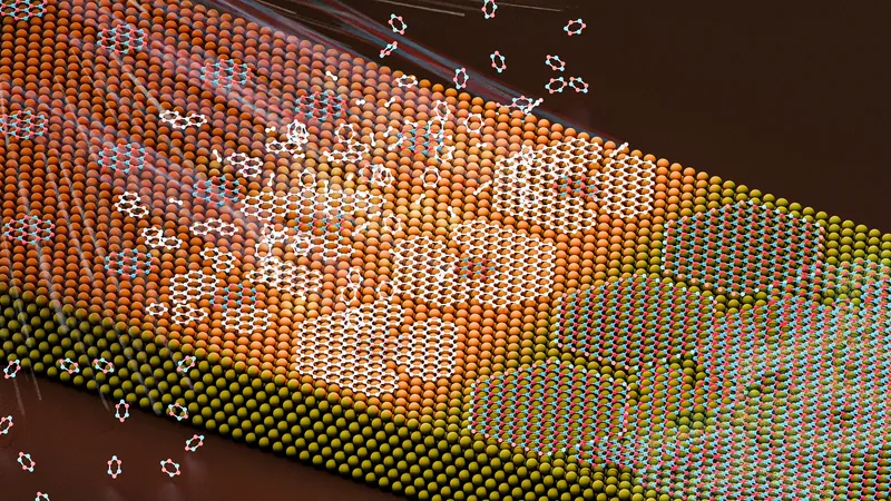
During this process, boron and nitrogen atoms are released to form triangular hBN islands on copper foil, which can grow larger and combine to create a continuous honeycomb lattice structure. However, Zhang and his team have optimized this CVD process by switching to hexagonal islands, resulting in superior quality films.
Role of Oxygen
Remarkably, introducing a trace of oxygen during the growth process plays a crucial role in the formation of these hexagonal islands. Researchers discovered that the presence of oxygen equalizes the stability of the boron and nitrogen edges, allowing them to grow at comparable rates.
Advanced Confirmation Techniques
Utilizing advanced techniques such as atomic force microscopy and high-resolution transmission electron microscopy, the team confirmed that this innovative method generates single-crystal hBN films that are free from pinholes, showcasing low defect densities, consistent thickness, and outstanding insulating properties.
Yield and Scalability
Impressively, the team successfully produced a 25 x 70 mm film of hBN, and with further developments, this process could yield even larger sheets suitable for industrial production.
Future Directions
As researchers delve deeper into the mechanisms behind the CVD growth of hBN, they aim to refine the quality and size of the films even further, paving the way for an exciting future in the realm of 2D materials and electronic devices.
Conclusion
Stay tuned for more updates on this potential game-changer in electronic manufacturing!


 Brasil (PT)
 Canada (EN)
 Chile (ES)
 España (ES)
 France (FR)
 Hong Kong (EN)
 Italia (IT)
 日本 (JA)
 Magyarország (HU)
 Norge (NO)
 Polska (PL)
 Schweiz (DE)
 Singapore (EN)
 Sverige (SV)
 Suomi (FI)
 Türkiye (TR)